
Digging into sync.Once: How Go Ensures One-Time Execution

· 7 min read
Prabhav Dogra
Software Engineer II @ Blinkit

How it started?

While writing some concurrent code for Blinkit, I found myself reaching for sync.Once—a common utility in Go to ensure an action is performed just once, no matter how many goroutines attempt it. Out of curiosity, I decided to dig into how sync.Once works internally and how its implementation has evolved over time. While investigating the internals I came across something interesting and ended up contributing myself — a small step, but super rewarding!

In this blog, I’ll walk through the internals of sync.Once, how it leverages atomics for performance, and trace its evolution through Go versions. This blog is meant to motivate you to explore and solve your own doubts by diving into the source code of Go itself. You’ll be amazed at how much you can learn just by following the code and seeing how things work behind the scenes!

Prerequisites: What's sync.Once?

  • sync.Once ensures a function is only executed once, no matter how many times it's called, even across goroutines.
  • It's most commonly used to initialize shared resources like config, DB connections, or singletons.
var (
readConfigOnce sync.Once
config *Config
)

func GetConfig() (c *Config) {
readConfigOnce.Do(func() {
// Read yaml and make config object
})
return config
}

func main() {
cfg := LoadConfig()
fmt.Println(cfg)
}

Link to sync.Once documentation

Digging into sync.Once internals?

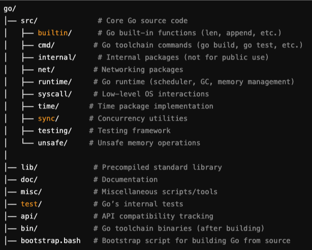
To follow along this read feel free to clone the Golang repository.

  • Open the repository and run the bash script ./make.bash, to build and install the latest compiler of Go.
  • Point your system or editor (like VSCode) to use the newly built Go version:
Bootstrapped Compilers

When I first came across the concept of a bootstrapped compiler, it honestly felt like a total brain teaser. The idea that a compiler could be written in the same language it’s supposed to compile? Wild.

Here’s the bombshell: the Go compiler is written in Go itself. Sounds paradoxical, right?

Like a classic chicken-and-egg dilemma - “How can a compiler compile itself if it doesn’t exist yet?”

In programming, bootstrapping refers to: The process of building a system using a simpler or initial version of itself.

  • make.bash is a shell script located at src/make.bash inside the Go source tree.
  • It's used to bootstrap the Go toolchain — it builds the Go compiler (cmd/compile), linker (cmd/link), and other core tools from scratch using the Go bootstrap toolchain.
  • It uses the already installed Go compiler
  • Use the clones Golang source code to build the new version of Go.

Internals (Go 1.18)

Let's start from the basics, struct of sync.Once looks like

src/sync/once.go | GOVERSION=1.18
type Once struct {
done uint32
m Mutex
}

Pretty simple, right?

  • One uint32 flag done
    • done == 1 means that the function has ran once
    • done == 0 means that the function hasn't ran yet
  • One mutex m
    • A mutex to avoid race condition while updating done

Ok, somehow these two are used together to:

  • Ensure that a particular action executes only once, regardless of how many times it is called concurrently.
  • Achieve this guarantee efficiently, minimizing lock contention for better performance.

Ok so far so good right?

Let's move to the implementation of once.Do(f): It ensures that the function f() is only executed once, no matter how many times it's called—even if from multiple goroutines.

src/sync/once.go | GOVERSION=1.18
func (o *Once) Do(f func()) {
if atomic.LoadUint32(&o.done) == 0 {
o.doSlow(f)
}
}

Goal: Avoid acquiring a mutex unless absolutely necessary (i.e., the function f() hasn’t run yet).

  • if atomic.LoadUint32(&o.done) == 0
    • We check if done == 0, done == 0 means that the function hasn't ran yet
    • It checks done == 0 atomically in one operation. More about atomic package
func (o *Once) doSlow(f func()) {
o.m.Lock()
defer o.m.Unlock()
if o.done == 0 {
defer atomic.StoreUint32(&o.done, 1)
f()
}
}
  • if o.done == 0
    • A second check inside the locked section.
    • Why? Because multiple goroutines might pass the atomic check in Do(), but only one should actually run the function. So we check again inside the lock to be 100% sure.
    • This is a double-checked locking pattern.
  • defer atomic.StoreUint32(&o.done, 1)
    • Marks the function as executed after f() is done.
    • It’s deferred so even if f() panics, we still consider it “done” and don't call it again (intentional in Go’s design).

Internals (Go 1.24)

In newer versions of Go they revised the implementation of how sync.Once.

src/sync/once.go | GOVERSION=1.24
type Once struct {
_ noCopy
done atomic.Uint32
m Mutex
}

Ok! What's changed now?

  • noCopy is embedded in Once struct
  • done is atomic.Uint32 not uint32

"noCopy" What's that?

  • It'a a zero-size struct that is adds no memory overhead.
  • Go has a statical analysis tool go vet that checks your Go source code for common mistakes and suspicious constructs that the compiler won’t catch.
  • Some types must never be copied once they’ve been initialized—most notably synchronization primitives like sync.Mutex, sync.Once, etc. Accidental copies can lead to deadlocks or data races.
  • Having noCopy embedded in your struct will produce a warning if your type is ever copied by go vet.

Regular uint32 vs. atomic.Uint32

When you don't know something in Go let's follow the approach like we have done, and let's look at the source code:

src/atomic/type.go | GOVERSION=1.24
type Uint32 struct {
_ noCopy
v uint32
}
  • Ok, wow! As you can see atomic.Uint32 is just a wrapper type around a uint32 with noCopy but why???

Let's look further functions binded to this struct:

// Load atomically loads and returns the value stored in x.
func (x *Uint32) Load() uint32 { return LoadUint32(&x.v) }

// Store atomically stores val into x.
func (x *Uint32) Store(val uint32) { StoreUint32(&x.v, val) }

// Swap atomically stores new into x and returns the previous value.
func (x *Uint32) Swap(new uint32) (old uint32) { return SwapUint32(&x.v, new) }

// CompareAndSwap executes the compare-and-swap operation for x.
func (x *Uint32) CompareAndSwap(old, new uint32) (swapped bool) { return CompareAndSwapUint32(&x.v, old, new) }

Ok, seems like it's just a wrapper type provides methods for atomic operations.

And that is exactly what atomic.Uint32 is:

A Go 1.19+ wrapper type around a uint32 that provides methods for atomic operations

Bonus: Go. 1.25 (Hopefully)

While exploring the internals of sync.Once, I noticed that the done field — which indicates whether the function has already been executed — was originally an atomic.Uint32.

However, since it’s only ever used as a boolean flag (0 or 1), I realized it could be more semantically clear to use atomic.Bool instead. Even though atomic.Bool is just a thin wrapper around a uint32 under the hood, switching to it makes the code more self-explanatory and aligns better with the intent of the field. So I decided to raise a PR and it got merged :)

Now the struct looks like this:

src/sync/once.go | GOVERSION=1.25
type Once struct {
_ noCopy
done atomic.Bool
m Mutex
}

Conclusion

Exploring sync.Once from Go 1.18 to Go 1.25 shows how a small, fundamental primitive can evolve for clarity, safety, and maintainability:

  • Go 1.18
    • Used a plain uint32 flag plus a Mutex and double‑checked locking
    • Minimized lock contention by atomically checking the flag on the fast path
  • Go 1.24

    • Embeds noCopy to catch accidental copies via go vet
    • Switches to atomic.Uint32, providing a clean, method‑based API
  • Go 1.25

    • Switches atomic.Uint32 to atomic.Bool

Along the way we’ve seen:

  • Bootstrapping – how Go builds itself from source via make.bash
  • Atomic vs. mutex – why lock‑free fast paths matter in high‑concurrency code
  • Static analysis – how noCopy and go vet help prevent subtle bugs

The beauty of Go’s standard library is that it balances performance, safety, and readability. Whenever you have a question about how Go works under the hood, the answer is just a GitHub clone and a make.bash away. Dive into the source, follow the code, and you’ll not only solve your doubts—you’ll discover deeper principles that make Go such a pleasure to work with.

And it’s downright fun to see how these technologies evolve over time.

What does memory mean actually?

· 12 min read
Prabhav Dogra
Software Engineer II @ Blinkit

Introduction

While exploring how Go manages memory, I stumbled upon an intricate hierarchy that determines how fast data moves between the CPU and RAM. Go’s runtime optimizations, like garbage collection and stack allocation, made me curious about what happens under the hood. This led me to registers, caches (L1, L2, L3), and RAM—each playing a crucial role in balancing speed and storage.

Prerequisites: What's a CPU Cycle?

CPU Cycle:

  • It's the smallest unit of processing that a CPU can do.
  • Each cycle allows the CPU to execute instructions like fetching data, performing arithmetic, or storing results.
  • For example: the method atomic.CompareAndSwap in go is executed as follows:
    • It reads a value from memory.
    • It compares it with an expected value.
    • If they match, it writes a new value.
    • This requires at least three steps (read, compare, write), which take multiple cycles.
  • A single 1GHz CPU can complete one CPU cycle in 1 nanosecond.
  • Similarly, a 3GHz CPU can complete one CPU cycle in 0.33 nanoseconds.
  • Not every operation takes 1 cycle
    • Simple instructions like integer addition (a + b) may take 1 cycle.
    • More complex operations (e.g., division, memory access) can take multiple cycles.

Clock edge

NOTE: Here Period = Clock Cycle

Clock edge A clock edge refers to the transition point of a clock signal where changes in a digital circuit occur. The clock signal is a periodic waveform (square wave), and it has two main edges:

  • Rising Edge (Positive Edge)
    • The transition from low (0) to high (1).
    • Many digital circuits, including registers and flip-flops, are designed to capture input and update their state on this edge.
  • Falling Edge (Negative Edge)
    • The transition from high (1) to low (0).
    • Some circuits use this edge for synchronization, though it is less common than the rising edge.

Why is the Clock Edge Important?

  • It synchronizes operations in digital circuits.
  • Registers and flip-flops capture and store data only on a specific edge, ensuring controlled data flow.
  • In CPU pipelines, clock edges trigger different stages like instruction fetch, decode, execute, etc.

Understanding Computer Memory Hierarchy

  1. Registers (Fastest, Smallest)
    • Located inside the CPU, closest to the execution units.
    • Stores data for immediate operations (e.g., arithmetic calculations).
    • Extremely small (few bytes) but operates at CPU clock speed.
    • Access time: 1 CPU cycle (fastest).
  2. L1 Cache (Level 1)
    • Smallest and fastest cache (typically 32KB to 128KB per core).
    • Directly integrated into the CPU core.
    • Stores frequently used instructions (will discuss this later) and data for ultrafast access.
    • Access time: 2-4 CPU cycles.
  3. L2 Cache (Level 2)
    • Larger than L1 (256KB to a few MB per core).
    • Slightly slower than L1 but still much faster than RAM.
    • Used to store recently accessed data that might be needed again soon.
    • Access time: 10-20 CPU cycles.
  4. L3 Cache (Level 3)
    • Shared among multiple CPU cores, ranging from a few MB to tens of MB.
    • Acts as a buffer between L2 and RAM, reducing latency for core-to-core communication.
    • Access time: 30-60 CPU cycles.
  5. RAM (Random Access Memory)
    • Main working memory for the system (GBs in size).
    • Much slower than CPU caches but holds more data.
    • Stores active processes and data that aren’t frequently used by the CPU.
    • Access time: 100+ CPU cycles.

Registers: The Fastest Storage

What Are Registers?

Registers are ultra-fast, small storage units embedded directly inside a computer’s CPU (Central Processing Unit). They are temporary holding areas for data, instructions, or memory addresses that the CPU needs to access immediately during computations. Registers are the fastest type of memory in a computer, designed to minimize delays in processing.

How Registers Work?

  • Fetching Data: When the CPU needs to perform an operation (e.g., 5 + 3), it first copies the values 5 and 3 from RAM into two registers.
  • Processing: The CPU’s arithmetic logic unit (ALU) performs the addition directly using the values stored in the registers.
  • Storing Results: The result (8) is placed into another register, which can either be used for further operations or written back to RAM.
  1. Basic Structure: Flip-Flops

    • Core Component: Registers are built using D-type flip-flops, each flip-flop just stores one bit. A 32-bit register, for example, contains 32 flip-flops.
    • Function: Each flip-flop has:
      • Data Input (D): Receives the bit to store.
      • Write Enable (WE): Controls whether the flip-flop should capture and store the input value on the next active clock edge.
      • Clock Input (CLK): Provides the timing signal that synchronizes when data is captured by the flip-flop. The flip-flop updates its value on the rising edge of the clock.
      • Output (Q): Provides the stored bit.
  2. Data Storage and Clock Synchronization

    Writing Data:

    • When the CPU writes to a register:
      • The write enable signal for the register is activated.
      • Data is placed on the input bus. The input bus is a set of electrical connections that carry data to the register.
      • In the next rising edge of the clock, the flip-flops capture the input values.

    Reading Data:

    1. Stored Data in Flip-Flops
      • A register consists of multiple flip-flops, each storing a single bit. Once a value is stored in a flip-flop, it remains available at its output until changed by a new write operation. However, this stored value is not automatically placed on the CPU’s internal bus—something must send the data when the data is read.
      • Each flip-flop's output is connected to a tri-state buffer, which controls whether the stored bit is driven onto the bus connecting CPU and register (for reading the bit).
    2. Role of the Tri-State Buffer
      • Tri-State Buffer ensures conflict-free (kindof like mutex) data access, enabling the CPU to perform billions of operations per second reliably.
      • A tri-state buffer is a special circuit that can either:
        • Tri-State Buffer Enabled: Passes the stored data from the register to the bus connecting CPU and register.
        • Tri-State Buffer Disabled: Disconnects the register from bus connecting CPU and register.
      • This is necessary because multiple registers share the same internal bus, and only one should be active at a time to avoid conflicting reads and writes (more of a hardware constraint).
      • The enable signal is synchronized with the CPU clock to ensure stable data transfer.

Types of Registers (A little extra context)

  • General-Purpose Registers:
    • Used for temporary data storage and most calculations.
  • Special-Purpose Registers:
    • Program Counter (PC): Holds the memory address of the next instruction to execute.
    • Instruction Register (IR): Stores the current instruction being decoded/executed.
    • Stack Pointer (SP): Tracks the top of the stack in memory.
    • Status/Flag Register: Stores metadata about operations (e.g., whether a result was zero or caused an overflow).

Why Registers Are Essential

  • Eliminate Bottlenecks: Without registers, the CPU would need to read/write data directly from RAM for every operation, which is too slow.
  • Enable Pipelining: Registers allow the CPU to work on multiple instructions simultaneously by holding intermediate states.
  • Direct Hardware Access: Registers interface directly with the CPU’s ALU and control unit, enabling rapid execution of machine-level instructions.

CPU Cache: L1, L2, L3 CPU caches

CPU Caches are small, ultra-fast memory layers between the CPU and main memory (RAM). They store frequently accessed data and instructions to reduce latency and improve performance. Modern CPUs use three levels of cache:

There are two types of cached instructions:

  • Instruction Cache:
    • What it stores:
      • Instructions are the actual binary code (machine code) of the program being executed by the CPU.
      • Examples: ADD, MOV, JUMP, LOAD, or any operation the CPU performs.
    • Purpose:
      • Allows the CPU to quickly fetch the next operation to execute.
      • For example, when running a loop, the instruction cache holds the repeated code (for, while loops) so the CPU doesn’t have to fetch it repeatedly from slower memory.
  • Data Cache:
    • What it stores:
      • Data refers to the values the CPU is actively working with.
      • Examples: Variables (e.g., int x = 5), memory addresses, temporary results, or input/output values.
    • Purpose:
      • Provides fast access to the operands (numbers, addresses) needed by instructions.
      • For example, when calculating x + y, the data cache holds the values of x and y for the ADD instruction to use.

Why Split Them?

  • Parallel Access:
    • The CPU can fetch the next instruction (from the instruction cache) while simultaneously reading/writing data (from the data cache). This avoids bottlenecks.
    • Example: While executing an ADD instruction, the CPU can already fetch the next instruction (MOV or JUMP) from the instruction cache.
  • Specialization:
    • Instruction caches are optimized for sequential access (program code is usually read in order).
    • Data caches are optimized for random access (variables can be accessed in any order).

L1 Cache (Level 1 Cache)

  • Role:
    • The fastest and smallest cache, directly integrated into the CPU core.
    • Split into L1 Instruction Cache (stores executable code) and L1 Data Cache (stores data).
  • Characteristics:
    • Size: Typically 32–64 KB per core (e.g., 64 KB total: 32 KB data + 32 KB instructions).
    • Speed: 1–4 clock cycles access time (fastest).
    • Location: Embedded within each CPU core.

L2 Cache (Level 2 Cache)

  • Role:
    • Acts as a middle layer between L1 and L3.
    • Stores data/instructions not held in L1 but likely to be reused.
  • Characteristics:
    • Size: 256 KB–2 MB per core (varies by CPU design).
    • Speed: 10–20 clock cycles access time.
    • Location: May be shared between cores or dedicated per core (e.g., AMD Zen vs. Intel Core).

L3 Cache (Level 3 Cache)

  • Role:
    • The largest and slowest CPU cache, shared across all cores.
    • Reduces traffic to RAM by storing data shared between multiple cores.
  • Characteristics:
    • Size: 4–64 MB
    • Speed: 20–50 clock cycles access time.
    • Location: On the CPU die but outside individual cores.

Why Three Levels?

  • Latency vs. Size Trade-off: L1 prioritizes speed for critical data, L2 balances speed and size, and L3 minimizes RAM access.
  • Efficiency: Reduces "cache misses" by filtering requests through layers (90% of data is often found in L1/L2).
  • Multicore Optimization: L3 enables shared data (e.g., game textures, OS tasks) to stay accessible to all cores.

Practical Example:

  • When running a game:
    • L1: Stores code for rendering a character (e.g., position calculations).
    • L2: Caches textures used in the current scene.
    • L3: Holds shared assets like audio files or global physics data.

Why not replace L2 and L3 with L1?

  • Physical Limits:
    • L1 is fast but bulky/power-hungry. Scaling it to L2/L3 sizes would make CPUs impractical (cost, heat, latency).
  • Hierarchy Efficiency:
    • L1: Speed-optimized for critical data.
    • L2: Balances size/speed for common data.
    • L3: Shared, large storage to minimize RAM trips.
  • Cache Miss Mitigation:
    • Without L2/L3, frequent RAM access (~100x slower) would cripple performance.
  • Power/Heat:
    • Larger L1 would drain power and overheat CPUs.
  • Multicore Sharing:
    • L3 allows cores to access shared data without duplicating it in L1/L2.

RAM: The Parts of the Memory Cell

Imagine a single memory cell in your computer’s RAM (the temporary memory your computer uses to do stuff). Think of it like a tiny light switch and a tiny battery working together to store a 0 or a 1 (the basic "yes/no" language computers use). Here’s how it works:

  • Capacitor: A tiny “battery” that can hold an electric charge.
    • Charged (has electricity) = 1
    • Not charged (empty) = 0
  • Transistor: A tiny “light switch” that controls access to the capacitor.
    • ON (switch closed) = Lets electricity flow.
    • OFF (switch open) = Blocks electricity.
  • Address Line: The wire that tells the transistor to turn ON/OFF.
  • Data Line: The wire that reads or writes the charge (0 or 1) to the capacitor.

How It Works

  1. Writing Data (Saving a 0 or 1)
    • Step 1: The CPU (computer’s brain) says, “Hey, I need to save a 1 at this specific memory cell!”
    • Step 2: The Address Line sends electricity (like flipping the switch ON).
    • Step 3: The Data Line sends electricity to charge the capacitor (filling the tiny battery). Result: Capacitor is charged = 1 is stored. If the CPU wants to save a 0, the Data Line drains the capacitor instead.
  2. Reading Data (Checking if it’s 0 or 1)
    • Step 1: The CPU says, “What’s stored at this memory cell?”
    • Step 2: The Address Line sends electricity (switch ON).
    • Step 3: If the capacitor is charged (storing 1), electricity flows out through the Data Line.
      • Result: The CPU detects this flow = 1.
    • Step 4: If the capacitor is empty (storing 0), no electricity flows.
      • Result: The CPU detects no flow = 0.

Refresh Cycle

  • Each DRAM cell consists of a capacitor (storing a 1 or 0 as charge) and an access transistor.
  • When a cell is “charged” (1) or “discharged” (0), that state is maintained only temporarily because the charge leaks away.
  • The DRAM controller (or memory controller) periodically reads each memory cell and then rewrites (recharges) it to restore the original value. This refresh cycle typically occurs every 64–128 milliseconds for all cells.
  • Without refreshing, the leakage would eventually cause the stored bits to flip, leading to data corruption. The periodic refresh ensures data integrity over time.

Writing your own Goroutines

· One min read
Prabhav Dogra
Software Engineer II @ Blinkit

This all started when someone asked me how goroutines work internally and all I could respond with was:

"Goroutines are lightweight threads managed by the Go runtime instead of the operating system. Go runtime automatically multiplexes—mapping multiple goroutines onto a smaller number of OS threads. And that somehow makes them fast?? 👉👈"

If anyone asked me any in-depth questions about how this multiplexing worked I was blank. So I decided to gain a deeper understanding by implementing goroutines myself. Cloned the Go Github repo

To be continued...

References

How Go atomic operations avoid race conditions?

· 5 min read
Prabhav Dogra
Software Engineer II @ Blinkit

Introduction

This question popped up in my head, "How Go atomic operations avoid race conditions?"

I finally gathered the courage to open the cloned Go Github repo and scan through it.

Go Code Structure

Go code structure

Source: ChatGPT

I went inside the implementation of CompareAndSwapInt32 and found this:

src/sync/atomic/doc.go
// CompareAndSwapInt32 executes the compare-and-swap operation for an int32 value.
// Consider using the more ergonomic and less error-prone [Int32.CompareAndSwap] instead.
//
//go:noescape
func CompareAndSwapInt32(addr *int32, old, new int32) (swapped bool)

Finding the implementation of this was not straightforward, because this method is implemented in Go Assembly:

src/sync/atomic/asm.s
TEXT ·CompareAndSwapInt32(SB),NOSPLIT,$0
JMP internal∕runtime∕atomic·Cas(SB)

What's Go Assembly?

Simply put, Go Assembly is the low-level language used to write performance-critical functions in Go. Go Assembler (Code directory path: cmd/asm) is the tool that compiles Go assembly (.s) files into machine code. The Go assembler was heavily inspired by the Plan 9 C compilers.

Plan 9 C compilers

Plan 9 C compilers (6c, 8c, 5c, etc.) were architecture-specific compilers designed to generate optimized code for different CPU architectures. Unlike GCC or LLVM, which support multiple architectures within a single compiler framework, Plan 9 used separate compilers for different instruction sets. These compilers were originally developed for the Plan 9 operating system, an experimental OS designed as a potential successor to Unix-based systems.

You can read more about it here: https://9p.io/sys/doc/compiler.html

Go drew inspiration from 9 C Compiler:

  • Just like Plan 9 had separate compilers for different architectures (e.g., 6c for x86-64, 8c for ARM, etc.).
  • Go’s assembler follows a similar architecture-based approach, instead of a universal assembler Go has different assemblers for x86, ARM, RISC-V, etc.

You can watch this, an interesting talk about Go Assembler presented by Rob Pike himself.

Go Assembler Documentation

Go Assembler streamlined a lot of things:

  • Portability: It abstracts CPU architecture details better.
  • Simpler syntax: No need for % prefixes, brackets, or complex addressing.
  • Unified across architectures: ARM, AMD64, RISC-V, etc., use the same structure.
  • Designed for the Go runtime: Helps implement Go features like garbage collection, goroutines, and stack growth efficiently.

Go Assembler has 4 architecture-specific implementations of atomic.CompareAndSwapInt32():

  • amd64.s: For AMD64 (x86-64) architecture (Intel, AMD CPUs).
  • arm64.s: For ARM64 (AArch64) processors (used in Apple M1/M2, mobile devices, servers).
  • ppc64le.s: For PowerPC 64-bit, Little Endian (used in IBM systems).
  • s390x.s: For IBM Z-series mainframes (used in enterprise computing).

Go runs on multiple architectures, and low-level atomic operations must be natively implemented for each to ensure compatibility.

Added the implementations for one architecture (other 3 are similar) in Go Assembly:

src/internal/runtime/atomic/atomic_amd64.s
// bool Cas(int32 *val, int32 old, int32 new)
// Atomically:
// if(*val == old){
// *val = new;
// return 1;
// } else
// return 0;
// }
TEXT ·Cas(SB),NOSPLIT,$0-17
MOVQ ptr+0(FP), BX
MOVL old+8(FP), AX
MOVL new+12(FP), CX
LOCK
CMPXCHGL CX, 0(BX)
SETEQ ret+16(FP)
RET

Explaining this line by line how this maintains atomicity.

TEXT ·Cas(SB),NOSPLIT,$0-17
  • TEXT ·Cas(SB): Declares the function Cas(CompareAndSwap) in Go assembly.
  • NOSPLIT: Instructs the runtime not to perform stack splitting, ensuring that the function runs without interruption. It tells the Go runtime not to perform stack splitting for that function.
  • $0-17: Specifies the stack frame size for the function (0 bytes for local variables and 17 bytes for arguments/return values).
MOVQ ptr+0(FP), BX:
  • Moves the pointer ptr (the address of val) from the function's frame pointer (FP) into the BX register.
MOVL old+8(FP), AX:
  • Moves the old value from the frame pointer into the AX register.
MOVL new+12(FP), CX:
  • Moves the new value from the frame pointer into the CX register.
LOCK:
  • This is a crucial instruction. It prefixes the next instruction (CMPXCHGL) with a lock, ensuring that the memory operation is atomic. This lock ensures that no other process or thread can modify the memory location while the compare and exchange instruction is running.
CMPXCHGL CX, 0(BX):
  • This is the Compare and Exchange instruction. It performs the following:
    • Compares the value in AX (the old value) with the value at the memory location pointed to by BX (the val value).
    • If the values are equal, it replaces the value at 0(BX) with the value in CX (the new value).
    • The original value at 0(BX) is loaded into the AX register.
SETEQ ret+16(FP):
  • SETEQ sets the byte at the destination to 1 if the zero flag is set, and to 0 otherwise. In this case, it sets the return value to 1 if the comparison was equal (meaning the swap was successful), and to 0 otherwise.
RET:
  • Returns from the function

Conclusion

At the register level, atomicity is achieved because:

  • The LOCK prefix serializes access across CPU cores.
  • CMPXCHGL ensures all three steps (compare, swap, write-back) happen as one unit.
  • The CPU guarantees atomicity, eliminating race conditions without software locks.

Feel free to be curious and figure out the answers to your questions on your own.

Building a Ray Tracer in C++

· 10 min read
Prabhav Dogra
Software Engineer II @ Blinkit

This blog is just a quick summary of the book Ray Tracing in One Weekend

Github Source Code: dograprabhav/ray_tracer

What're we gonna make?

Final

Milestone 1:

Before starting anything, in this milestone we just create a sample image. To do that we use one of the simplest formats P3. P3 is a plain text format for Portable Pixmap (PPM) image files. It is one of the simplest image formats, where pixel data is represented in plain text.

P3 Image Format

In P3, each pixel is defined by three integers corresponding to the red, green, and blue color channels. The first line of the output is "P3", identifying the file format. The second line contains the width and height of the image. The third line specifies the maximum color value (typically 255, representing the maximum intensity for each color channel). Each subsequent line contains three integers (r, g, b) for each pixel's color in the image.

Sample P3 image of width 2 pixels and height 3 pixels
P3           // Defining format
2 3 // Width and Height
255 // Maximum color value
2 5 15 // (r, g, b) color intensity triplets
0 255 255 // (r, g, b) color intensity triplets
255 0 255 // (r, g, b) color intensity triplets
255 255 0 // (r, g, b) color intensity triplets
0 0 0 // (r, g, b) color intensity triplets
255 255 255 // (r, g, b) color intensity triplets

This image looks like:       P3

Milestone 1 Results

We write a simple loop to render this:

P3

Milestone 2:

In this milestone we setup a basic ray tracing setup.

  • We setup a sphere in the scene.
  • We setup light rays that detects object in the scene.
  • On the basis of intersection of light rays and objects in the scene it detects what each pixel in the image should look like.
  • Set up vector ray header files

How it works?

How it works? This image represents the basic concept of a ray-tracing camera model used in computer graphics and rendering. Let’s break it down step by step:

  • Camera and Viewport Setup: The camera center is the origin of the coordinate system. A viewport (camera screen/a plane) is placed in front of the camera at a certain focal length. The viewport is divided into a grid of pixels (X × Y), where each cell represents a pixel in the final rendered image.

  • Ray Tracing Process: For each pixel in the viewport grid

    • A ray of light is cast from the camera center through the center of the pixel.
    • The ray travels in the scene and intersects with objects (like the blue sphere in the diagram).
    • If a ray hits an object, the rendering algorithm calculates the color of that pixel based on:
      • The material properties (color, reflectivity, transparency).
      • Lighting conditions (shadows, reflections, refractions).
      • Camera perspective.
    • The computed color is assigned to the corresponding pixel in the final image.

Sphere-Ray Intersection

This section explains the mathematical derivation for determining the intersection points between a ray and a sphere.

Sphere Equations

  • Sphere centered at (0, 0, 0):
    • x² + y² + z² = r²
  • Sphere centered at (Cx, Cy, Cz):
    • (Cx - x)² + (Cy - y)² + (Cz - z)² = r²

Vector and Distance

  • Vector from point A(x1, y1, z1) to B(x2, y2, z2):
    • (B - A) = (x2 - x1, y2 - y1, z2 - z1)
  • Distance between points A and B:
    • d = √[(x2 - x1)² + (y2 - y1)² + (z2 - z1)²]
  • Vector from point P(x, y, z) to center C(Cx, Cy, Cz):
    • (C - P) = (Cx - x, Cy - y, Cz - z)

Point on Sphere Condition

For point P to lie on the sphere, it must be 'r' (radius) distance from the center:

  • (C - P) ⋅ (C - P) = (Cx - x)² + (Cy - y)² + (Cz - z)²
  • (Cx - x)² + (Cy - y)² + (Cz - z)² = r² (Distance from center)
  • Therefore: (C - P) ⋅ (C - P) = r²

Ray Equation

  • General ray equation: RAY(t) = M * t + N
    • M is the ray's direction vector.
    • N is the ray's origin point.

Ray-Sphere Intersection

A ray hits the sphere when it's 'r' distance from the center:

  • (C - RAY(t)) ⋅ (C - RAY(t)) = r²
  • (C - (M * t + N)) ⋅ (C - (M * t + N)) = r²
  • Expanding the equation:
    • t² * M ⋅ M - 2 * t * M ⋅ (C - N) + (C - N) ⋅ (C - N) - r² = 0

Quadratic Formula

Using the quadratic formula (roots = -b ± √(b² - 4ac) / 2a), we get:

  • a = M ⋅ M
  • b = -2 * M ⋅ (C - N)
  • c = (C - N) ⋅ (C - N) - r²

By solving this quadratic equation for 't', we can find the intersection points (if any) between the ray and the sphere.

Milestone 2 Results

Milestone 2 results

Milestone 3:

  • Scene Abstraction:
    • Introduced a Scene structure to manage all objects, lights, and properties in the environment.
    • Simplifies the rendering process by treating the scene as a collection of objects instead of handling each separately.

Result: The code is cleaner, modular, and easier to extend in the future (e.g., adding reflections, refractions, and different shapes).

Milestone 3 Results

Milestone 3 results

Milestone 4:

Rendering Improvements

  • Added Anti-Aliasing
    • Reduced jagged edges in the final image by averaging multiple rays per pixel.
  • Added Camera Class
    • Abstracted camera logic for better scene control.
  • Started Considering Reflected Rays
    • Introduced initial logic for reflection to create mirror-like surfaces.
    • Prepares the system for handling realistic light behavior.

Material System Enhancements

  • Added Material Class for Diffuse Material
    • Defined a reusable Material class to manage object properties.
    • Simplified code structure by encapsulating material behavior.
  • Added Material Class with Diffuse Material
    • Implemented Lambertian reflection for diffuse surfaces.
    • Ensures objects interact naturally with light sources.
  • Added True Lambertian Reflection
    • Improved light scattering on rough surfaces.
    • Used a more accurate random sampling technique for diffuse reflections.
  • Gamma Correction
    • Gamma Correction for More Realistic Colors

Anti-aliasing

  • Reduced jagged edges in the final image by averaging multiple rays per pixel. Anti-Aliasing

A Simple Diffuse Material

A diffuse surface is a surface that scatters light in many directions instead of reflecting it in a single, well-defined direction (like a mirror). This happens because the surface is rough at a microscopic level.

  • Some observations:
    • A light ray that bounces of a diffuse surface has equal probability of bouncing in all directions
    • They might also be absorbed rather than reflected. The darker the surface, the more likely the ray is absorbed (that’s why it's dark!).
  • How we will do it:
    • Generate a random vector inside the unit sphere
    • Normalize this vector to extend it to the sphere surface
    • Invert the normalized vector if it falls onto the wrong hemisphere

Generating randomised reflected rays

True Lambertian Reflection

A more accurate representation of real diffuse objects is the Lambertian distribution. This distribution scatters reflected rays in a manner that is proportional to cos(𝜙), where 𝜙 is the angle between the reflected ray and the surface normal.

This means that a reflected ray is most likely to scatter in a direction near the surface normal, and less likely to scatter in directions away from the normal. We do this by

src/v4/camera.h
    // rec.normal is the normal to the hemisphere
vec3 direction = rec.normal + random_unit_vector();

Gamma Correction

  • Gamma Correction for More Realistic Colors
    • Raw pixel values in the renderer are stored in linear color space.
    • Most displays, however, interpret color values in a non-linear way, requiring gamma correction.
    • Gamma correction is applied using the equation:
    corrected color = raw color ^ (¹⁄ᵧ)
    where γ (gamma) is typically 2.2.

Milestone 5:

Metal

  • Add a new class to Material class for Metal object
  • Modelled light scatter and reflectance, enabling realistic surfaces.
  • Added mirrored light reflection for metallic objects.
  • Implemented fuzzy reflection, simulating rough metallic finishes.

Dielectrics

  • Explored refraction and how light bends through transparent materials.
  • Used Snell’s Law to determine how rays change direction at surfaces.
  • Introduced total internal reflection, where light stays within the medium.
  • Implemented the Schlick Approximation for realistic reflection intensity.

Positionable Camera

  • Defines camera viewing geometry for perspective accuracy.
  • Introduces controls for positioning and orienting the camera, improving scene setup.

Metallic Surfaces and Reflective Rays

Introduces metallic materials by modifying how rays bounce off surfaces. Reflection is modeled using the equation:

𝑅 = 𝑉 − 2 (𝑉 ⋅ 𝑁) 𝑁 

Mirrored reflection

  • Where,
    • 𝑅 is the reflected ray,
    • 𝑉 is the incoming ray, and
    • 𝑁 is the surface normal. The reflected ray is traced to determine the color contribution from the metal.
  • Fuzziness in Reflection:
    • To simulate rough metal, a fuzziness parameter is introduced.
    • Instead of perfect reflection, a small random offset is added to the reflected ray direction.
    • The amount of fuzziness controls how polished or rough the surface appears.

Dielectrics

Clear materials such as water, glass, and diamond are dielectrics. When a light ray hits them, it splits into a reflected ray and a refracted (transmitted) ray. We’ll handle that by randomly choosing between reflection and refraction, only generating one scattered ray per interaction.

Snell's Law

Where 𝜃 and 𝜃′ are the angles from the normal, and 𝜂 and 𝜂′ are the refractive indices. The geometry is:

⇒ 𝜂 ⋅ sin𝜃 = 𝜂′ ⋅ sin𝜃′

where:

  • 𝜂 — Refractive index of the first medium
  • 𝜂′ — Refractive index of the second medium
  • 𝜃 — Incident angle (angle between the incoming ray and the normal)
  • 𝜃′ — Refracted angle (angle between the refracted ray and the normal)

Snell's Law

Total Internal Reflection

Total Internal Reflection (TIR) occurs when light traveling from a denser medium to a less dense medium is completely reflected rather than refracted. This happens when the angle of incidence exceeds the critical angle, given by:

theta = sin⁻¹(n₂ / n₁)

TIR

Schlick's Approximation

Schlick's Approximation provides an efficient way to estimate reflectance at the interface of two materials based on the angle of incidence.

schlicks

R₀ = ((n₁ - n₂) / (n₁ + n₂))²

This approximation avoids expensive computations while providing visually accurate reflections.

Final Render

Final